
Packaging for mmWave Devices — Why Do We Need It, and How Do We Do It?
By Liam Devlin, CEO, Plextek RFI

Why is it desirable to use semiconductor devices in surface-mount (SMT) packages rather than as bare die? After all, an unpackaged chip would be smaller and would have lower parasitics, giving better performance.
The answer is that packaged devices are much easier to handle and are compatible with high-volume manufacturing and assembly techniques. Unpackaged die need specialist handling in a cleanroom environment, and it is difficult to solder other components to a circuit board that includes bare die. So, the chips contained in any commercial product intended to be produced in reasonably high numbers likely need to be in suitable packages.
As 5G creates a volume demand for ICs at millimeter wave (mmWave) frequencies, it creates additional packaging challenges. The packages’ physical dimensions become a significant fraction of a wavelength, which can cause resonance issues. Bond wire parasitics always need to be taken into account but, at higher frequencies, the impact of the inductive parasitics can severely impact performance — thus, the bond wires need to be considered as an integral part of the circuit.
Several package types can be used at mmWave frequencies, all with their own strengths and weaknesses, so the choice will depend on the specific application. However, some general design rules apply to all forms of packaging.
First, it is necessary to think of how the package will interact with both the die and the PCB. The key to successful packaging is co-design of the IC and the package, in order to optimize the performance of the packaged device rather than that of the chip on its own. It is important to begin by matching the die size with the size of the package, which will keep the bond wires as short as possible and reduce their inductance.
Bond wire parasitics can also be reduced by using two or even three bond wires in parallel, which requires a larger bonding pad on the IC. The increased capacitance of this larger pad can help improve the RF performance of the package transition by forming a low pass filter in combination with the bond wire inductance. Optimizing the capacitance at the PCB is also useful, as this forms the other end of the filter.
Overmolded plastic packaging is the ‘workhorse’ of low-cost, high-volume manufacturing. It is based upon a leadframe: a thin sheet of metal with many device footprints etched out on it. The die is normally attached using conductive epoxy, then the bond wires are added to the pads, and the whole device is encapsulated in a plastic molding compound. The addition of the molding compound also introduces losses and dielectric loading, which must be accounted for as part of the design process.
Many IC processes include passivation of the chip, and this can help to mitigate the effect of the molding compound. With mmWave ICs, electromagnetic (EM) simulation is always used as part of the design process, and this optimization should include the molding compound.
The packaged device will need to be mounted on a PCB, requiring careful design. The PCB substrate should not be too thick, as this makes it dispersive at higher frequencies — its propagation characteristics vary with frequency. The use of a thin substrate also helps reduce grounding inductance and improves thermal performance. Most mmWave plastic-packaged ICs have an exposed die-attach paddle that must be connected to the PCB ground. An array of vias is used to do this, and a thin substrate can help to keep this effective grounding inductance low. Should the grounding inductance be too high, feedback can occur around the IC that would degrade performance and ultimately cause stability issues.
Since this inductance increases with both frequency and gain, the effect becomes increasingly pronounced at mmWave frequencies, making a low-inductance ground connection essential. Most commercially available SMT packaged mmWave amplifiers have a gain of around 20 – 25 dB; mmWave amplifiers with levels of gain higher than this are likely to encounter problems when housed in an SMT package.
For some applications, a custom leadframe can be used, offering features that make it easier to use at higher frequencies. By grounding some of the unused pins directly to the die-attach paddle, the integrity of the ground connection can be enhanced, which reduces grounding inductance and improves the transition from the RF ports to the IC. Overmolded packages are routinely used up to 30 – 35 GHz but, depending on the IC functionality, they can work well to even higher frequencies.
Air cavity plastic packages appear similar to overmolded ones, but they incorporate an air cavity above the chip, reducing the molding compound’s effects on device performance. Although this type of package incurs a tooling charge, it potentially offers better RF performance at the higher mmWave frequencies and has been successfully used by Plextek RFI to realize of power amplifiers at frequencies up to 43 GHz. Fig. 1 shows a comparison of an overmolded plastic package and an air cavity package, both of which are in a 5 mm x 5mm quad flat no-leads (QFN) configuration.
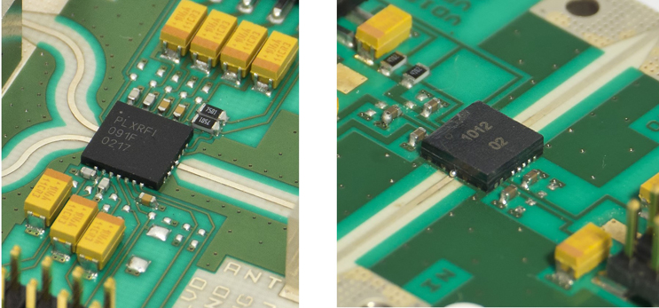
Fig. 1 — (left) an overmolded 5mm x 5mm QFN plastic package containing a 28GHz FEM and (right) an air-cavity 5mm x 5mm QFN package containing a 39GHz PA
There is also a range of ceramic packages available commercially that are open-tooled, and these have been demonstrated to work well up to 40 GHz. With a solid metal base and an air cavity, the IC can be designed to fit the package dimensions to provide optimum RF performance for the packaged part. Although they are considerably more expensive than plastic packages, particularly in low volumes, the costs reduce considerably as quantities increase.
An advantage of ceramic packages is that they are more robust environmentally and have the potential to be made hermetic. Custom versions can be designed, but a standard package with proven RF performance is a popular option. Many of the open-tooled ceramic packages are in a QFN format, the most common approach for mmWave.
Laminate packages can also be in QFN format. A potential advantage of this package type is that it can be customized internally to fit the size of an existing die design. The die sits in an internal well with its top surface at almost the same height as the level that will be bonded to, which allows bond wires to be kept short.
It is also particularly suitable for mounting multiple die in the same package (Fig. 2), as it allows routing between the chips and even the incorporation of integral filtering, which can be included at no extra cost. SMT laminate packages have been used for commercial products at frequencies up to 45 GHz.
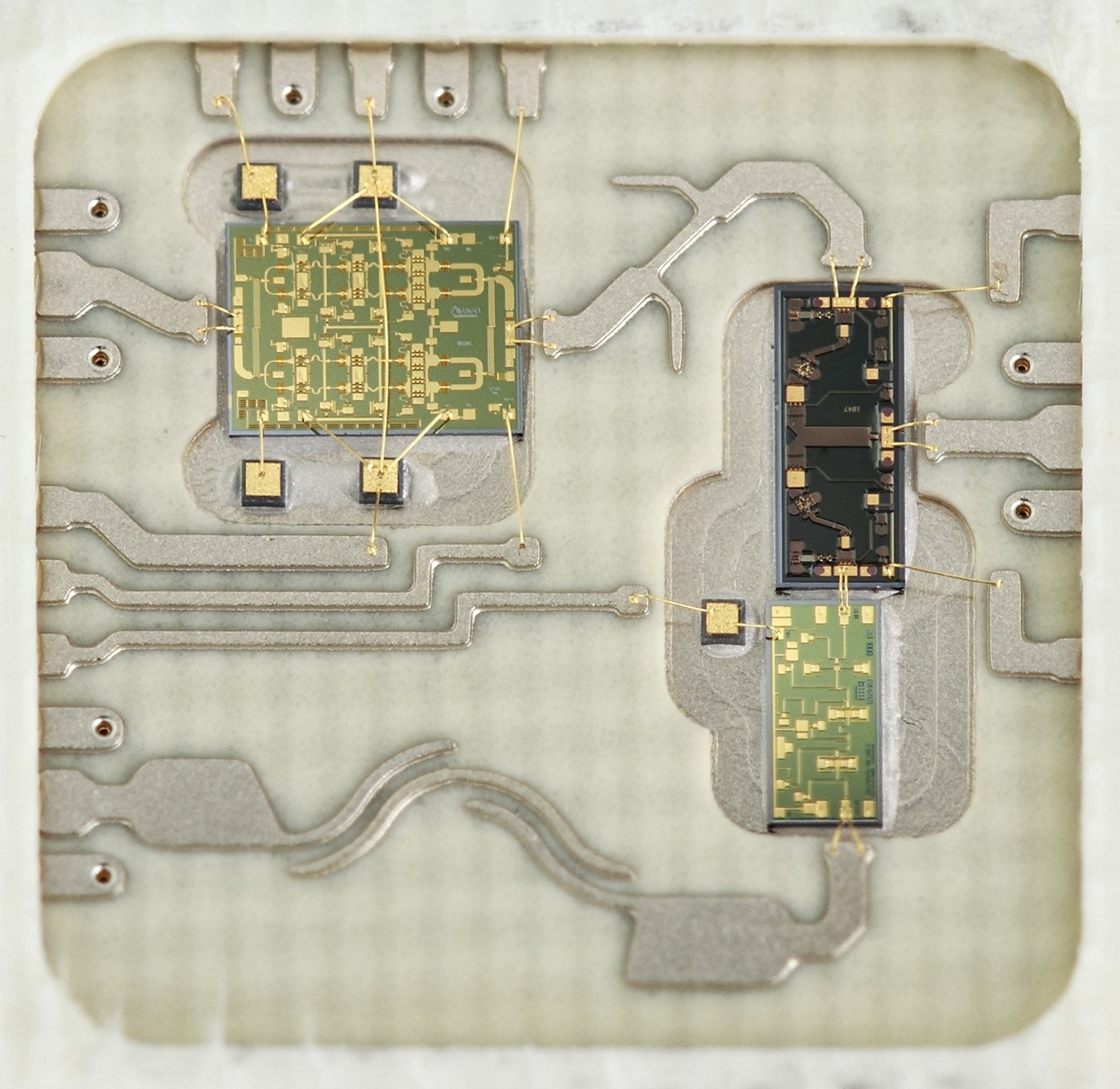
Fig. 2 — 10 mm x 10 mm QFN laminate package containing three-chip 26 GHz FEM with integral filtering
Wafer Level Chip Scale Packaging (WL/CSP) is more common with silicon ICs than with GaAs. In the final stage of processing a “redistribution level” is added, which provides some routing on the top of the chip, and the base of the chip-scale package itself. The IC is then flipchipped to form the package, which reduces the RF bond inductance and allows low inductance connections from the top side of the IC to ground. Unlike GaAs chips, Si ICs do not have intrinsically low inductance to the substrate ground, so flipchipping is almost universally used as a means of connecting Si RF ICs into a package with low parasitics.
Finally, Antenna in Package (AiP) can be a useful technique, as this removes the need for an RF port to a PCB, resulting in a very compact design. This can incorporate an array of antennas, which can be combined in a phased array approach. It has the advantage of offering a lot of functionality in a compact footprint and could be an attractive solution for mmWave 5G consumer products. Its disadvantage is that it is very application-specific, and there’s no facility to add additional filtering outside the package, so all the filter requirements need to be included internally.
The importance and the challenges of implementing production test of mmWave ICs should not be underestimated. All these package types need a special fixture for testing that minimizes the parasitics it adds and allows measurements to be calibrated to the package reference planes. A suitable load board must also be developed to present realistic operating conditions for the test.
In conclusion, mmWave packaging presents some unique challenges to the MMIC designer. The associated parasitics can lead to severe degradation at these frequencies, but with careful design this can be mitigated, and it is possible to produce SMT packaged devices that give excellent performance in the volumes that will be required for 5G applications.
About the Author
Liam Devlin is the CEO of Plextek RFI, a UK-based design house specializing in the design and development of RFICs, MMICs, and microwave/mmWave modules. He has led the design and development of over 100 custom ICs on a range of GaAs, GaN, and Si processes at frequencies from baseband to 90 GHz, and has also developed microwave and mmWave sub-systems using a variety of technologies. Liam previously worked as Chief Designer for Marconi Caswell, and was employed by Philips Research Laboratories. Liam has a BEng in Electrical and Electronic Engineering from the University of Leeds, UK.