
Inductorless Regulators Deliver Negative Bias to GaAs Power Amps

Engineers employing GaAs amplifiers can turn to boost/buck regulators to reduce size and cost while increasing talk time in their handset designs.
By: Patrick Maresca, Product Manager for Wireless Applications, TelCom Semiconductor
As wireless handsets move further into the consumer space, designers need to implement RF products, such as power amplifiers and switches, that can deliver high performance, low cost, and small size. To achieve these goals, wireless designers have traditionally turned to CMOS and bipolar CMOS (Bi-CMOS)-based chip solutions for their products.
Although silicon products deliver low cost solutions to the wireless market, they do have some drawbacks. In particular, silicon products generally don't deliver the performance levels required by wireless systems operating in the GHz range, such as those used by PCS systems.
To solve these performance hurdles, engineers have turned to GaAs components for their higher frequency wireless products. And, with wireless applications continuing to move up the frequency band, the need for GaAs components will continue to be prevalent in future wireless markets.
Bias supply requirements
To properly bias a GaAs power amplifier (PA), a negative DC bias is required. There are many methods for providing this DC bias, but in a majority of applications, a regulated bias scheme is desirable over an unregulated inverting charge pump (Figure 1).
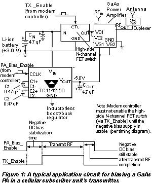
The inductorless voltage inverter is the core of the negative DC bias generator. It is a switched capacitor (charge pump) voltage converter that only requires two 0.47 µF flying capacitors and a 4.7 µF output capacitor to operate. The voltage inverter's output ripple magnitude is dependent on the three external capacitors. The output ripple waveform is superimposed on the nominal -5.0 VDC and has a fundamental frequency of 200 kHz.
In the past, many designers have chosen a switching regulator to operate with a GaAs PA. That trend is changing. Recent technology developments have swayed many engineers toward using inductorless regulators in their handset designs.
Since switching regulators require inductors, they increase the installed size, generated noise, and cost of providing a negative DC bias. Inductorless regulators, on the other hand, provide a "boost/buck" regulated conversion from either a single-cell lithium-ion (Li-ion), a multi-cell nickel cadmium (NiCd), or a multi-cell nickel metal hydride (NiMH) battery pack.
Ordinary charge pumps simply invert (not regulate) their input voltages. For example, TelCom Semiconductor's (Mountain View, CA) TC7660 charge pump generates a no-load output voltage of –5 VDC when VIN = +5 VDC. However, its output voltage falls with a corresponding decrease in input voltage, an increase in output current, or both.
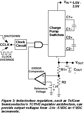
Regulated charge pumps, such as TelCom's TC1142, differ in that they use pulse-frequency modulation control to generate a regulated output voltage without the use of a post linear regulator. For example, the TC1142 consists of an inverting/doubling charge pump and a feedback circuit (sampling resistors R1, R2, /ERROR comparator, and associated voltage reference). When operating at full clock speed, the charge pump generates an unregulated output voltage equal to -2VIN.
The /ERROR comparator inhibits operation of this charge pump (i.e. skips clock pulses) whenever the output voltage sampled by R1 and R2 is more negative than the internal reference voltage. This combination of the doubling charge pump and feedback regulation scheme allows the absolute value of VOUT to be regulated above or below that of VIN (hence, boost/buck operation). For example, the TC1142 delivers an output voltage of –5 VDC at a maximum load current of 20 mA over an input voltage range of +2.5 to +5.5 VDC.
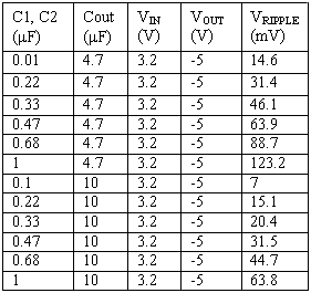
In order to maintain the lowest output resistance and output ripple voltage, engineers should employ low equivalent series resistance (ESR) capacitors in their designs. In addition, larger values of the output capacitor and lower values of the flying capacitors will also reduce the output voltage ripple.
Depending on the required size of the capacitors, the inductorless regulating charge pump also provides more than adequate regulation for most portable applications. The table below shows the relationship between output voltage ripple versus the two flying capacitors (C1 and C2) and the output capacitor (COUT). In each case, a +3.2 VDC input is being converted to a –5 VDC output.
Assuming the output is loaded to at least 20% of the maximum available current, the power efficiency of the inductorless boost/buck regulator can be estimated as the absolute value of the regulated voltage, divided by twice the input voltage. Thus, for a +3.6 VDC single cell Li-ion battery input generating a –5 VDC output, the efficiency of the inductorless boost/buck regulator will be approximately 70%. This increased efficiency leads to decreased power consumption and increased talk time in a handset design.
Devising clever methods to extend the talk time in a handheld subscriber units (when a GaAs PA is active) is always a key challenge for the design engineer. It is interesting to note that as the battery voltage decreases to +3 VDC, the efficiency of the inductorless boost/buck operation increases to approximately 80%. This improved efficiency further decreases power consumption and increases talk time in a cellular or PCS mobile phone.
Wrap up
GaAs has become the technology of choice over silicon in cellular telephone power amplifier applications. With GaAs technology, lower noise figures, higher cutoff frequencies, and higher power-added efficiency allow the cellular user increased talk time as compared to silicon PAs. GaAs PAs require a negative DC bias, and inductorless boost/buck regulating charge pumps offer significant advantages over inductor-based switchers or unregulated charge pumps. By turning to inductorless regulators in a handset design, engineers can achieve lower generated noise, smaller installed size, lower installed cost, and excellent output regulation.
About the author:
Pat Maresca, Product Manager for Wireless Applications, TelCom Semiconductor, Inc., 1300 Terra Bella Avenue, Mountain View, CA 94043. Phone: 650-968-9241 ext. 839; Fax: 650-967-1590.