
Changes in PLL Parameters Impact Receiver System Performance

By: Dean Banerjee, Wireless Applications Engineer, National Semiconductor
Contents
Lock time
Reference spurs
Phase noise
The phase locked loop (PLL) has become an essential component in the design of receivers for both wireless infrastructure and handset designs. As a result, engineers must have a proper understanding of these products when developing their wireless receivers.
When evaluating PLLs, receiver designers need to evaluate many key parameters, such as lock time, reference spurs, and phase noise, and reference spurs. In particular, engineers must determine how these parameters will affect the general system performance of a typical receiver.
A block diagram of a typical receiver architecture is displayed in Figure 1. In this example there are 79 channels with center frequencies starting at 2.402 GHZ and ending at 2.480 GHz, which are spaced 1 MHz apart.

In the above example, let's suppose that a channel with frequency 2.45 GHz is received. This signal goes through the preselection filter and the first PLL (PLL1), where it is tuned to 2.25 GHz, exactly 200 MHz below the signal value to be received. The 200 MHz difference frequency as well as the sum of the frequencies at 2650 MHz enter the bandpass filter. Only the 200 MHz signal passes through the filter and low-noise amplifier (LNA) to the second PLL (PLL2). The second PLL is always tuned at 200 MHz, and recovers the demodulated data, which is sent to the baseband processing.
Keep this above example in mind because the rest of the article will use this figure as an example below to show how PLL parameters affect overall system design.
Lock time
In a PLL design, lock time is the time that it takes the PLL to switch from one frequency to another for a given frequency change to a given frequency tolerance. For many cellular and cordless phones, this is typically in the order of several hundred microseconds.
In the time that the PLL takes to switch frequencies, data cannot be transmitted. Therefore, having too long of a lock time in the PLL can reduce the data rate of the system. For example, the Bluetooth standard says that a system can hop up to 1600 hops/s. In this case, the PLL can stay on a channel only 625 µs. This means that that the PLL lock time can be only a fraction of 625 µs. If this lock time is not achieved, the system will wait too long for the PLL to switch frequencies and, in turn, will achieve lower data rate levels.
In Figure 1 above, PLL2 is tuned to a fixed frequency. Thus, lock time will most likely not be an issue. Since this lock time requirement in this portion of the receive chain is typically not very stringent, engineers can turn to PLLs with a relatively narrow loop bandwidth. By employing this type of PLL, engineers can achieve lower phase error and spurious emissions.
The lock time requirements of PLL1, however, are greatly different. In a typical receiver architecture, the first PLL is generally tunable so that the receiver can adjust to changing frequencies when a user becomes faded or interference is present in the channel. If a quick lock time is not achieved by PLL1, overall receiver performance can be degraded.
Reference spurs
Reference spurs are spurious emissions that occur from the carrier frequency at an offset equal to the channel spacing. These spurs are usually caused by leakage and mismatch in the charge pump of a PLL. Although the reference spurs usually occur outside of the band of interest, they can enter the mixers and be translated back onto the band of interest.
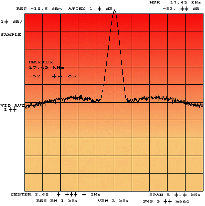
Using the receiver depicted in Figure 1, let's consider what happens when in addition to producing the desired 2.25 GHz carrier, PLL1 produces spurious sidebands that are spaced at a 1 MHz offset from the carrier. These sidebands would be at 2.224 MHz and 2.226 MHz. Now suppose that in addition to the desired carrier to be received at 2450 MHz, there is another user on the system at who is transmitting a signal at 2451 MHz, and this signal at 2451 MHz is much stronger than the signal at 2450 MHz. The other user's signal at 2451 MHz can mix with the spur at 2226 MHz, and produce a frequency of 200 MHz, which will interfere with the desired signal.
This is just one possible way that reference spur can cause a problem. In a transmitter, reference spurs can cause interference in a similar way.
For PLL2, the loop bandwidth is often chosen to minimize root-mean-square (RMS) phase error. Although the optimal RMS phase error loop bandwidth is application specific, it is typically on the order of 1 kHz or so.
The channel spacing for PLL2 may not be intuitively obvious in this example. This spacing, however, should be chosen equal to the greatest common multiple of the output frequency/frequencies and the crystal reference frequency used. PLL2 channel spacing is typically much larger than the loop bandwidth, therefore making reference spurs much less challenging for PLL2. This is perhaps the one reason for why it is getting more popular to integrate the functionality of PLL2 into application-specific ICs (ASICs).
Phase noise
The phase noise spectral density of a PLL system refers to the noise power of the PLL versus the offset frequency. Close to the carrier, within the loop bandwidth of the PLL, this noise is commonly dominated by the phase detector of the PLL. Further out, phase noise is typically dominated by the voltage-controlled oscillator (VCO; Figure 2).
If the carrier signal has phase noise around it, then the carrier from an undesired user in the system can mix with this noise and produce an unwanted spur at the desired carrier frequency. This is why standards often dictate a spectral mask requirement, which gives the maximum phase versus frequency offset for the carrier.
In a receiver subsystem, PLL phase noise can also contribute to RMS phase error. For a noisy sinewave, the zero crossings of the signal will not always occur at the reference period of the signal, but will actually statistically vary from this with a mean of zero and a standard deviation equal to the RMS phase error. If the RMS phase error is sufficiently large, then it can cause the symbol that is sent to be misinterpreted as a different symbol.
The quadrature phase shift keying (QPSK) constellation diagram below shows the relative phases of the in-phase (I) and quadrature (Q) signals (Figure 3). Each point on the constellation diagram corresponds to a different symbol, which could represent multiple bits.
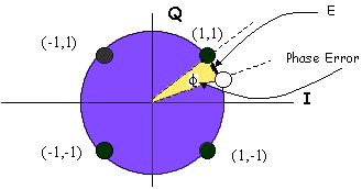
Consider an ideal system in which the only noise-producing component is the PLL in the receiver. In this example, the symbol corresponding to the bits (1,1) is the intended message indicated by the darkened circle. However, because the PLL has a non-zero RMS phase error contribution, the received signal is actually the non-filled circle.
If this experiment was repeated, an engineer would discover that that the phase error between the received and intended signal is normally distributed with a standard deviation equal to the RMS phase error. If the RMS phase error of the system becomes too large, it could actually cause a message to be interpreted as ( -1, 1) or ( 1,-1 ).
To determine the affect of phase noise, engineers can use the following formula:
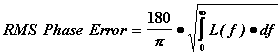
In the above formula, the phase noise, L(f), is proportional to the voltage noise squared. By integrating this voltage noise over the frequency band of interest and applying the square root, engineers can determine the RMS error for the zero crossings of the voltage signal. This value is then converted from radians into degrees.
Overall, the phase noise of PLL1 tends to be more critical and challenging to meet than the phase noise of PLL2. The reason for this is that PLL1 must tune over all 79 channels, while PLL2 only has to tune to a single frequency. Sometimes, PLL2 is adjusted to compensate for different Federal Communication Commission (FCC) requirements in different countries, but it is not changed once this is done. For these reasons, the loop bandwidth of PLL1 is typically wider than that for PLL2, and therefore there is a larger RMS error contribution.
References:
Banerjee, Dean: PLL Performance, Simulation, and Design, 1998,
Bluetooth Website: http://www.bluetooth.com
Christian Olgaard, Bill Burdette and William O. Keese: An In-Loop Modulation Synthesizer for Constant Envelope Digital Communication Systems
Vikas Vinayak, William O. Keese, and Christopher Lam: A 2.4 GHz Radio Solution for Bluetooth and Wireless Home Networking. Presented at September 1999 Wireless Symposium
About the author:
Dean Banerjee, Wireless Applications Engineer, National Semiconductor Corp., 1090 Kifer Rd. MS 16-177, Sunnyvale, CA 94086. Phone: 408-721-3319, Fax: 408-721-5559.